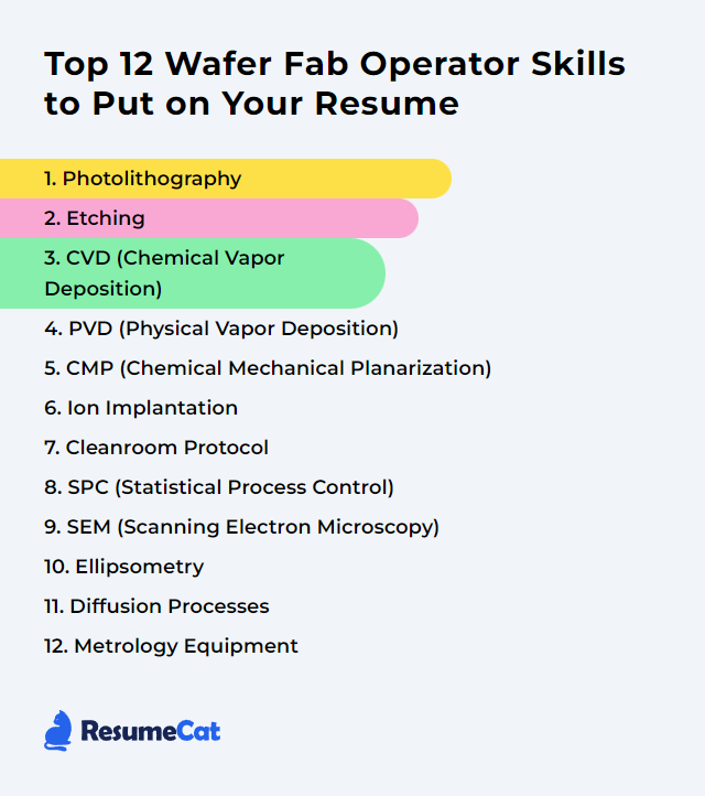
Top 12 Wafer Fab Operator Skills to Put on Your Resume
In today's semiconductor race, standing out as a wafer fab operator means proving you can run precise processes, keep yields up, and solve problems fast. A resume that showcases the right mix of technical depth and steady cleanroom habits signals you’re production-ready and worth the interview.
Wafer Fab Operator Skills
- Photolithography
- Etching
- CVD (Chemical Vapor Deposition)
- PVD (Physical Vapor Deposition)
- CMP (Chemical Mechanical Planarization)
- Ion Implantation
- Cleanroom Protocol
- SPC (Statistical Process Control)
- SEM (Scanning Electron Microscopy)
- Ellipsometry
- Diffusion Processes
- Metrology Equipment
1. Photolithography
Photolithography transfers patterns from a reticle onto a photoresist-coated wafer using light exposure and development, creating the fine features needed for downstream steps.
Why It's Important
It defines critical dimensions and overlay that ultimately set device performance and yield. Miss here, and everything downstream pays for it.
How to Improve Photolithography Skills
To strengthen litho performance on the floor:
Resolution and pattern fidelity: Apply resolution enhancement techniques like optical proximity correction and phase-shift strategies. For advanced nodes, understand immersion and EUV constraints, dose/focus windows, and stochastics.
Resist process control: Match resist to wavelength and target CD. Tighten coat uniformity, bake profiles, and development time to curb footing, scumming, and line-edge roughness.
Exposure optimization: Tune focus-exposure matrices, tighten overlay budgets, and use advanced alignment recipes. Where needed, leverage double/multi-patterning.
Tool health: Keep scanners/calibrations current—illumination uniformity, stage mapping, alignment mark cleanliness, and lens contamination checks.
Contamination control: Guard resist lines, filters, and track modules. Scrub particles at every handoff; monitor defects and haze rigorously.
Process control: Use SPC on CDs, overlay, and defectivity. Close the loop fast with metrology feedback and recipe tweaks.
Dial these in and patterns print cleaner, tighter, more repeatable.
How to Display Photolithography Skills on Your Resume
2. Etching
Etching uses wet chemistries or plasma to selectively remove material from wafers, shaping lines, vias, and high-aspect features.
Why It's Important
It sculpts device geometry and interfaces. Etch bias, profile control, and selectivity make or break device performance.
How to Improve Etching Skills
Sharper etch results come from disciplined control:
Recipe tuning: Balance gas flows, RF power, pressure, and time to hit target profiles and CD. Guard selectivity and sidewall passivation.
Chamber condition: Maintain seasoning, chamber wall state, and hardware health to reduce drift and micro-masking.
Mask quality: Feed the chamber good patterns—resist/hardmask integrity matters for line-edge roughness and critical dimensions.
Environment stability: Keep temperature and humidity consistent to stabilize etch rates and resist behavior.
In-line inspection: Use post-etch metrology and quick defect scans to catch bowing, notching, and footing early.
Advanced methods: Apply atomic layer etching (ALE) where ultra-precise control or sensitive interfaces demand it.
Operator training: Strengthen troubleshooting and fault recovery to minimize scrap when excursions pop up.
Consistency is king; stable chambers, stable outcomes.
How to Display Etching Skills on Your Resume
3. CVD (Chemical Vapor Deposition)
CVD deposits thin films from reactive gases onto wafers, producing conformal layers used for dielectrics, conductors, and barriers.
Why It's Important
Film quality—uniformity, stress, composition—directly impacts device reliability and electrical behavior.
How to Improve CVD (Chemical Vapor Deposition) Skills
Push film quality and throughput by focusing on:
Process window: Fine-tune temperature, pressure, and flow ratios. Monitor in real time; lock in stable nucleation and growth.
Tool care: Clean chambers on schedule, verify mass flow controllers and thermocouples, and track drift.
Precursor purity: Use high-purity chemistry and correct storage/handling to lower defectivity and contamination.
Variants: Use PECVD for low-temp films, LPCVD for uniformity, HDP-CVD for gap-fill—the right method for the job.
Training and SOPs: Keep recipes, interlocks, and safety steps tight; refresh skills routinely.
Stable films, fewer reworks, happier yields.
How to Display CVD (Chemical Vapor Deposition) Skills on Your Resume
4. PVD (Physical Vapor Deposition)
PVD deposits thin films by sputtering or evaporation, laying down metals, barriers, and seed layers.
Why It's Important
Adhesion, resistivity, step coverage, and film stress set the tone for interconnect reliability and downstream patterning.
How to Improve PVD (Physical Vapor Deposition) Skills
Better coatings without the headaches:
Recipe refinement: Balance power, pressure, target-substrate distance, and substrate temperature to tune stress and microstructure.
Hardware upkeep: Keep targets conditioned, shields clean, and pumps leak-tight. Calibrate rate monitors and thickness gauges.
Surface prep: Clean wafers thoroughly; add plasma pre-clean steps when adhesion is touchy.
Material quality: High-purity targets curb particles and inclusions. Track lot-to-lot variability.
In-situ monitoring: Use rate/thickness feedback and endpoint checks to stabilize deposition.
Skills and safety: Train on vacuum practices, target changes, and arc handling. Fewer surprises; safer shifts.
Uniform films mean smoother downstream CMP and litho.
How to Display PVD (Physical Vapor Deposition) Skills on Your Resume
5. CMP (Chemical Mechanical Planarization)
CMP polishes wafers with slurry and pads to flatten surfaces, enabling precise multilayer stacking.
Why It's Important
Planarity and surface quality protect device integrity and litho focus. Bad dishing or erosion translates into parametric drift.
How to Improve CMP (Chemical Mechanical Planarization) Skills
Nail consistency and defect control:
Pad conditioning: Keep pad texture within spec to stabilize removal rates and reduce scratch risk.
Slurry control: Use the right chemistry, flow rates, and filtration. Watch pH and particle stability.
Pressure/velocity: Tune downforce, platen/carrier speeds, and carrier backing pressure to control non-uniformity.
Endpoint and metrology: Apply in-situ sensors or timed polish backed by post-CMP thickness checks.
Preventive maintenance: Replace consumables on schedule; keep lines clean and seals healthy.
Clear SOPs: Standardize recipes and handling; train for rapid defect response and slurry anomalies.
Less scratching. Better flatness. Stronger yield.
How to Display CMP (Chemical Mechanical Planarization) Skills on Your Resume
6. Ion Implantation
Ion implantation accelerates ions into silicon to dope regions with precise doses and energies, setting junction depths and profiles.
Why It's Important
It controls electrical behavior at a granular level. Accurate implants mean consistent devices and reliable performance.
How to Improve Ion Implantation Skills
Make implants sharp and stable:
Dose and energy: Tune to achieve target sheet resistance and junction depth; validate with metrology.
Beam control: Monitor beam current, uniformity, and scan patterns; mitigate channeling with tilt/rotation and amorphization steps when needed.
Equipment health: Keep electrostatics, scanners, and source parts maintained. Calibrate dosimetry frequently.
Thermal management: Use wafer cooling and manage thermal loads to avoid resist/wafer damage.
Masks and alignment: Protect sensitive regions and ensure pattern fidelity with accurate alignment.
Post-implant anneal: Coordinate activation anneals (RTA/furnace) to repair damage and activate dopants without excessive diffusion.
Precision in, precision out.
How to Display Ion Implantation Skills on Your Resume
7. Cleanroom Protocol
Cleanroom protocol is the disciplined set of behaviors, garments, and handling rules that keep particles, chemicals, and ESD from wrecking wafers.
Why It's Important
Contamination kills yield. Strong protocol slashes defects and erratic parametrics.
How to Improve Cleanroom Protocol Skills
Tighten the chain from door to tool:
Training refreshers: Reinforce gowning, tool entry, and contamination awareness regularly.
Proper gowning flow: Follow the exact don/doff order. Replace worn garments; verify fit and coverage.
Tool and material handling: Clean, bag, and stage materials correctly. Wipedowns before entry. Antistatic practices always.
Cleaning cadence: Keep surfaces, benches, and equipment on strict cleaning schedules; verify with particle counts.
Air quality: Monitor particle levels, temperature, humidity, and pressure differentials. Maintain HEPA/ULPA integrity.
Flow control: Define personnel/material paths to cut cross-contamination. Limit traffic where it matters.
Audits and monitoring: Run routine audits and respond fast to excursions with root cause and retraining.
Small habits, big impact.
How to Display Cleanroom Protocol Skills on Your Resume
8. SPC (Statistical Process Control)
SPC applies statistical methods to monitor process variation in real time and keep production inside control limits.
Why It's Important
It catches drifts early, trims scrap, and stabilizes performance. Fewer surprises, tighter distributions.
How to Improve SPC (Statistical Process Control) Skills
Make data work for you:
Education: Ensure operators understand control charts, capability (Cp/Cpk), and basic problem-solving.
Real-time data: Automate collection from tools and metrology. Trigger alerts on rule violations.
Standard work: Document processes to reduce special-cause variation; keep change control strict.
Calibration: Maintain measurement systems; run MSA studies to ensure good data.
Effective software: Use SPC dashboards that surface trends quickly and support drill-down.
Continuous improvement: Close the loop with corrective actions, Kaizen events, and verified fixes.
Root cause rigor: Apply 5 Whys/Fishbone thoughtfully; prevent recurrence with hard controls.
Good SPC turns noise into signal.
How to Display SPC (Statistical Process Control) Skills on Your Resume
9. SEM (Scanning Electron Microscopy)
SEM provides high-resolution images of wafer surfaces and cross-sections to spot defects, measure features, and verify processes.
Why It's Important
It’s the microscope that reveals what optical tools miss—line edge roughness, voids, residues, subtle profile errors.
How to Improve SEM (Scanning Electron Microscopy) Skills
Sharper images, faster insights:
Sample prep: Keep surfaces clean; cleave carefully; avoid charging with proper grounding or coatings as appropriate.
Instrument setup: Calibrate regularly. Optimize accelerating voltage, probe current, working distance, and aperture.
Imaging technique: Balance resolution and beam damage. Use appropriate detectors (SE/BSE) and scan speeds.
Image processing: Adjust contrast/brightness thoughtfully and apply minimal filtering to retain detail.
Repeatability: Standardize recipes for routine measurements to ensure apples-to-apples comparisons.
See more, guess less.
How to Display SEM (Scanning Electron Microscopy) Skills on Your Resume
10. Ellipsometry
Ellipsometry measures thin film thickness and optical constants by tracking polarization changes upon reflection.
Why It's Important
Non-destructive, precise, and fast—ideal for controlling deposition and oxidation steps without wrecking wafers.
How to Improve Ellipsometry Skills
Solid measurements come from disciplined practice:
Calibration: Regular instrument checks—light source, detector response, angle alignment.
Environment: Stabilize temperature and minimize vibration for repeatable results.
Sample prep: Clean surfaces thoroughly; fingerprints and residues skew models.
Model accuracy: Use appropriate optical models and updated n/k libraries; validate with cross-techniques when possible.
Operator proficiency: Train on fitting strategies, goodness-of-fit metrics, and limits of the technique.
Good modeling turns raw data into trustworthy numbers.
How to Display Ellipsometry Skills on Your Resume
11. Diffusion Processes
Diffusion drives dopants into silicon under controlled temperature and atmosphere to form junctions and tailor conductivity.
Why It's Important
It creates the p-n structures at the heart of devices, with junction depth and concentration profiles steering performance.
How to Improve Diffusion Processes Skills
Control the furnace, control the profile:
Thermal uniformity: Verify zone uniformity and ramp profiles; map regularly to reduce across-wafer variation.
Gas delivery: Keep mass flows stable and clean; monitor oxygen, nitrogen, or dopant sources precisely.
Pre-clean: Use strong pre-diff cleans to strip metals/organics; cleaner surfaces yield better uniformity.
Time/temperature: Optimize for dopant species and target junctions; validate with SIMS or sheet resistance checks.
Atmosphere control: Choose oxidizing/inert ambients intentionally to manage oxide growth and dopant behavior.
Calibration and maintenance: Keep thermocouples, pyrometers, and gas lines accurate and leak-free.
Advanced tools: Use RTP for short, sharp thermal budgets to limit diffusion while activating dopants.
SPC discipline: Track key parameters and react quickly to drift.
Stable profiles, predictable devices.
How to Display Diffusion Processes Skills on Your Resume
12. Metrology Equipment
Metrology tools measure thickness, CDs, overlay, topography, and defects to verify every step is holding spec.
Why It's Important
Quality isn’t guessed—it’s measured. Accurate metrology keeps processes honest and products consistent.
How to Improve Metrology Equipment Skills
Sharper data, better decisions:
Regular calibration: Reference certified standards; run periodic verification routines.
Software and recipes: Keep analysis software current. Standardize measurement locations and sampling plans.
Automation: Use automated handlers and sequences to reduce operator variability and increase throughput.
Environmental control: Stabilize temperature, humidity, and vibration near sensitive tools.
Operator training: Build competency in gauge R&R, uncertainty, and tool-specific nuances.
Preventive maintenance: Follow strict PM schedules—optics clean, stages aligned, sensors validated.
Trustworthy measurements fuel real process control.
How to Display Metrology Equipment Skills on Your Resume