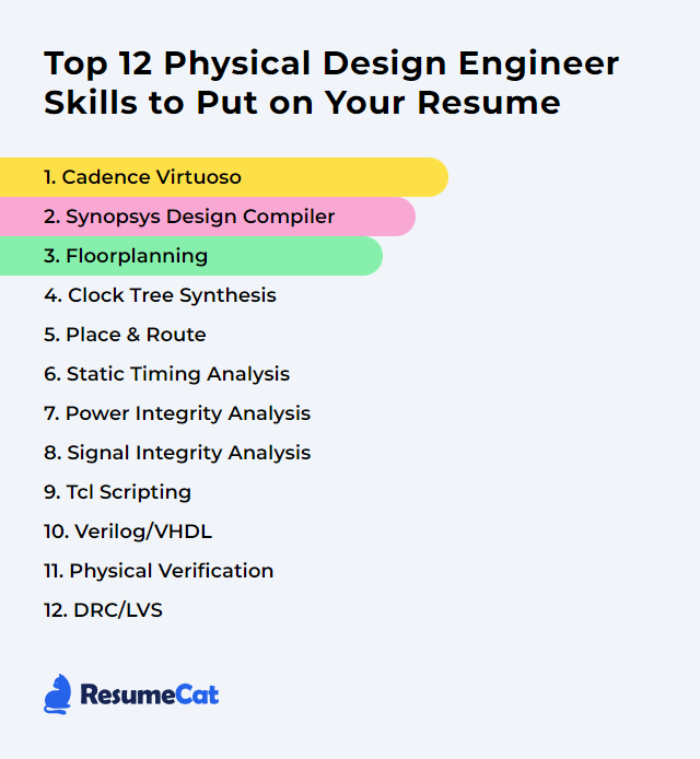
Top 12 Physical Design Engineer Skills to Put on Your Resume
In the competitive world of physical design engineering, the right skills on your resume can swing doors open. Targeted, practical, demonstrable abilities. The kind that move silicon from intent to tapeout without drama. Below, a sharp rundown of 12 essentials that help you stand out where it counts.
Physical Design Engineer Skills
- Cadence Virtuoso
- Synopsys Design Compiler
- Floorplanning
- Clock Tree Synthesis
- Place & Route
- Static Timing Analysis
- Power Integrity Analysis
- Signal Integrity Analysis
- Tcl Scripting
- Verilog/VHDL
- Physical Verification
- DRC/LVS
1. Cadence Virtuoso
Cadence Virtuoso is a comprehensive platform for custom, analog, and mixed-signal IC design—schematic capture, simulation, layout, and verification stitched together so you can move fast without losing precision.
Why It's Important
Virtuoso gives a Physical Design Engineer the canvas and the instruments to craft and validate silicon at fine granularity, enabling accurate layout, efficient iteration, and reliable signoff for high-performance chips.
How to Improve Cadence Virtuoso Skills
Level up by mixing fundamentals with automation and steady practice.
Nail the essentials: Shortcuts, editors, constraint-driven layout, parameterized cells. Read the official docs and actually try the workflows.
Automate with SKILL: Write snippets to eliminate repetitive clicks—naming, checks, device swaps, layout generation. Small scripts compound.
Layout craft: Focus on floorplanning, routing strategies, guard rings, shielding, matching, and clean DRC/LVS practices.
Keep current: New PCells, device models, extraction options, and reliability checks appear often. Track release notes and team playbooks.
Community and reviews: Share utilities with peers, run design reviews early, and borrow proven conventions across projects.
Consistency pays—tight loops of practice, feedback, and refinement make Virtuoso feel frictionless.
How to Display Cadence Virtuoso Skills on Your Resume

2. Synopsys Design Compiler
Synopsys Design Compiler translates RTL into an optimized gate-level netlist, balancing power, performance, and area while honoring constraints and preparing designs for physical implementation.
Why It's Important
Synthesis choices ripple downstream. Solid DC work improves correlation, shortens timing closure, and reduces ECO churn during P&R and signoff.
How to Improve Synopsys Design Compiler Skills
Perfect your constraints: Clean, complete SDC—clocks, IO delays, clock groups, false and multicycle paths, derates. Garbage in, grief out.
Script with intent: Modular, readable Tcl flows with checkpoints and reports. Target critical paths and avoid time-sink options for non-critical logic.
Hierarchy strategy: Choose flattening vs. preservation wisely. Partition for reuse, compile time, and better physical correlation.
Physical awareness: Use physical guidance and correlate with place-and-route (e.g., Design Compiler Graphical or handoff to Fusion Compiler/IC Compiler II) to reduce surprises.
Recovery loops: After initial P&R, feed back timing to re-synthesize hot spots with tuned constraints and targeted optimization.
Stay trained: Tool options evolve; new switches and engines can unlock measurable PPA gains.
Good synthesis isn’t just faster—it’s cleaner downstream.
How to Display Synopsys Design Compiler Skills on Your Resume
3. Floorplanning
Floorplanning sets the physical blueprint of a chip—macro placement, keepouts, channels, IO ring strategy, and resource allocation that tame congestion and timing before they become problems.
Why It's Important
Great floorplans shorten wires, calm clocks, and make routing civilized. Weak ones create timing traps, IR headaches, and chaos you fight for weeks.
How to Improve Floorplanning Skills
Define constraints early: Aspect ratio, core utilization, macro orientations, halos, pin placement, and routing corridors. Front-load decisions.
Power, clock, thermals: Budget strap grids, tap cells, clock entry points, and thermal escape paths alongside macro layout.
Connectivity-aware macro placement: Cluster by communication intensity and timing sensitivity; minimize detours and cross-traffic.
Iterate with data: Use trial route and early congestion/timing reports to reshape the plan. Don’t wait for full route to learn the lesson.
IP discipline: Align IP placement with bus fabrics, PHY proximity, analog keepouts, and ESD considerations.
Review rhythm: Regular check-ins against spec—timing, area, power targets—and adjust before inertia sets in.
How to Display Floorplanning Skills on Your Resume

4. Clock Tree Synthesis
Clock Tree Synthesis builds and balances the distribution network so clock edges arrive when they should, with controlled skew and jitter and power that doesn’t run away.
Why It's Important
The clock is the heartbeat. If skew or insertion delay is off, timing slips and power climbs. CTS keeps the design honest.
How to Improve Clock Tree Synthesis Skills
Target skew and jitter: Choose suitable topologies, insert and size buffers thoughtfully, and balance loads to flatten surprises.
Hierarchy matters: Build a tree of trees—global, regional, local—so latency is predictable and ECOs don’t ripple everywhere.
Use the right engine: Perform CTS in place-and-route tools (e.g., Synopsys Fusion Compiler or IC Compiler II, Cadence Innovus) for realistic physical correlation.
Power-smart tactics: Clock gating, useful skew, and buffer pruning reduce dynamic and leakage without gutting margins.
Plan in floorplan: Reserve sites and routing for spines and buffers to avoid last-minute congestion wrestling.
Post-CTS checks: Re-run timing, EM/IR, and noise. Validate with accurate extraction and fix hot spots iteratively.
Tool literacy: Learn the knobs—balancing, slew targets, shielding options, and CTS ECO flows. Siemens EDA, Synopsys, and Cadence docs are valuable.
How to Display Clock Tree Synthesis Skills on Your Resume
5. Place & Route
Place & Route transforms the netlist into a manufacturable layout, solving for timing, congestion, crosstalk, and design rules while meeting power and area constraints.
Why It's Important
This is where intent becomes geometry. P&R quality sets the tone for timing closure, power integrity, and yield.
How to Improve Place & Route Skills
Start with a disciplined floorplan: Hierarchical planning, realistic utilization, and room for clock and power structures.
Power planning first: Strong grids, uniform strap patterns, tap cells, and decap strategy to curb IR and Ldi/dt noise.
Placement that thinks ahead: Timing-driven, congestion-aware placement. Leverage modern placers in IC Compiler II or Fusion Compiler, Innovus, and similar tools.
CTS done right: Integrate CTS with placement realities; avoid over-buffering and keep shielding sane.
Routing with integrity: Handle shielding for sensitive nets, spacing to reduce coupling, layer budgeting, and antenna fixes. Calibre (Siemens) and foundry decks guide the rules.
Post-route polish: ECOs for late timing, crosstalk repair, hold fixes, and leakage recovery.
Timing signoff loop: Correlate with PrimeTime and golden extraction; feed back deltas for clean closure.
Verify relentlessly: Frequent DRC/LVS and density checks to avoid endgame surprises.
How to Display Place & Route Skills on Your Resume

6. Static Timing Analysis
Static Timing Analysis verifies that every timing path meets setup and hold requirements across modes and corners—no vectors required, just constraints, models, and math.
Why It's Important
STA is the safety net before tapeout. It catches violations early, informs fixes precisely, and builds confidence in silicon behavior.
How to Improve Static Timing Analysis Skills
Constraint hygiene: Accurate clocks, IO delays, exceptions, uncertainty, and derates. Keep them versioned and reviewed.
Design for timing: Drive synthesis and placement with timing in mind—gate sizing, buffering, retiming, and restructuring where it counts.
CTS tuning: Control skew and insertion delay; anchor critical domains and verify after every significant change.
Advanced effects: Use OCV/AOCV/POCV, crosstalk analysis, aging corners, and realistic RC extraction for believable results.
Focused fixes: Separate setup vs. hold workflows. Use incremental STA to accelerate iterations and measure impact.
Tight collaboration: Align with RTL, synthesis, and P&R owners so fixes don’t fight each other.
How to Display Static Timing Analysis Skills on Your Resume
7. Power Integrity Analysis
Power Integrity Analysis checks that the PDN delivers stable voltage everywhere—managing IR drop, dynamic droop, and noise so logic behaves under stress.
Why It's Important
Unreliable power wrecks timing and can trigger functional errors. Solid PI protects performance, reliability, and yield.
How to Improve Power Integrity Analysis Skills
Model faithfully: Use accurate library, package, and board models. Garbage modeling leads to false confidence.
Decap strategy: Place and size decoupling capacitors near hungry blocks and along noisy paths to tame transients.
Grid design: Engineer strap width/pitch, via farms, and domain partitioning for even distribution and manageable IR.
Simulate early and often: Run static and dynamic IR analyses with representative vectors and corner conditions (tools like SIwave, RedHawk, Voltus, and equivalents).
Mitigate IR and EM: Widen metals, add vias, rebalance domains, and adjust switching profiles. Track electromigration margins.
Thermal coupling: Heat shifts resistance and behavior. Co-analyze thermal maps with PI results to avoid hot spot traps.
Iterate with signoff data: Use post-route extraction and realistic activity to refine late-stage fixes.
How to Display Power Integrity Analysis Skills on Your Resume

8. Signal Integrity Analysis
Signal Integrity Analysis evaluates whether signals survive their journey—timing, noise, reflections, and coupling all in check so data lands cleanly.
Why It's Important
High speeds and dense routing invite crosstalk and distortion. SI discipline keeps interfaces robust and logic trustworthy.
How to Improve Signal Integrity Analysis Skills
Accurate models: Use proper IBIS/Spice models, stackups, and via models. Align with foundry and package data.
Reduce crosstalk: Space aggressors, route differential pairs tightly, use shielding on the truly critical lines, and watch for long parallel runs.
Power integrity synergy: Cleaner PDN equals quieter references—decaps and plane strategies help SI, too.
Right terminations: Series, parallel, or on-die termination chosen to control reflections and meet eye margins.
Simulate early: Pre-route what-if analysis; post-route with extracted parasitics for reality checks.
Layout discipline: Length matching, via count control, return path continuity, and sensible layer usage.
Keep learning: Materials, packaging, and speeds change. Refresh methods as technologies move.
How to Display Signal Integrity Analysis Skills on Your Resume

9. Tcl Scripting
Tcl is the glue for EDA flows—automation, reporting, mass edits, and tool customization that turn hours into minutes.
Why It's Important
Automation crushes repetition and cuts error rates. Tcl lets you shape tool behavior and build reproducible, portable flows.
How to Improve Tcl Scripting Skills
Master the core: Lists, dicts, procs, control flow, file I/O, regular expressions. Simple, powerful, everywhere.
Know your tool APIs: Cadence, Synopsys, and Siemens EDA expose rich Tcl commands—study the reference guides for your daily tools.
Automate real work: Start with reporting and rule checks, then scale to constraint generation and ECO automation.
Structure and reuse: Write libraries, add logging, and handle errors cleanly. Make scripts composable.
Debug and profile: Print wisely, isolate issues, and optimize hotspots. Small fixes can slash runtime.
Community habits: Share snippets within your team and keep a curated toolbox you can carry project to project.
How to Display Tcl Scripting Skills on Your Resume

10. Verilog/VHDL
Verilog and VHDL describe digital hardware. They let you model, simulate, and synthesize behavior into structures that tools can place and route.
Why It's Important
Clean RTL is the seed of clean silicon. Good code styles translate into easier synthesis, tighter timing, and fewer ECO fires.
How to Improve Verilog/VHDL Skills
Foundations first: Data types, blocking vs. non-blocking, processes, resets, parameterization, packages. Clarity over cleverness.
Relentless practice: Build small to medium designs—FIFOs, arbiters, CDC bridges, AXI components—then simulate and lint.
Synthesis-friendly style: Keep combinational vs. sequential logic clean, avoid latches, and respect timing implications of coding choices.
Simulate like you mean it: Constrained random where useful, assertions, and coverage to catch corner cases before synthesis.
Tool fluency: Get comfortable with ModelSim/Questa, Vivado, Quartus, and signoff flows so you understand how code becomes gates.
Community and reviews: Code reviews, style guides, and shared libraries lift quality quickly.
How to Display Verilog/VHDL Skills on Your Resume
11. Physical Verification
Physical Verification checks your layout against rules and intent—DRC for manufacturability, LVS for connectivity, plus antenna and density checks to keep foundries happy.
Why It's Important
Catching violations before tapeout avoids expensive respins. It’s the last sanity check that design matches rules and design matches schematic.
How to Improve Physical Verification Skills
Automate checks: Script repeatable DRC/LVS runs with structured reports and waiver tracking.
Use current decks: Keep foundry rule files updated; stale decks create churn and false confidence.
Incremental verification: Verify changed regions frequently to maintain velocity and reduce big-bang surprises.
Cross-verify when needed: Where possible, compare results across engines (e.g., Siemens Calibre and other verification tools) to shore up edge cases.
Clean layout habits: Label nets, organize hierarchy, and enforce layout conventions to accelerate debug.
Tight collaboration: Sync with foundry contacts and internal teams to resolve ambiguous rules or corner violations quickly.
Keep learning: New nodes, new rules—stay sharp with training and internal knowledge bases.
How to Display Physical Verification Skills on Your Resume
12. DRC/LVS
DRC (Design Rule Check) enforces foundry geometry rules. LVS (Layout Versus Schematic) ensures the layout matches the intended connectivity. Together, they guard manufacturability and correctness.
Why It's Important
Skipping rigor here is how respins happen. DRC/LVS keeps the layout legal and faithful to the design.
How to Improve DRC/LVS Skills
Know the rulebook: Study the process design rules and common pitfalls for the node you’re taping out.
Strong libraries: Use well-qualified, technology-matched libraries to avoid systemic violations.
Run early, run often: Incremental checks during layout curb pileups at the end.
Prefer clean IP: Pull in DRC/LVS-clean IP whenever possible to reduce noise.
Automate fixes: Script recurring corrections and waiver processing to accelerate closure.
Cross-check tools: When feasible, validate with more than one checker to catch corner issues.
Share context: Keep designers, layout engineers, and verification teams aligned on rule interpretations and ECO impacts.
Stay current: Track updates from vendors like Cadence, Synopsys, and Siemens EDA.
How to Display DRC/LVS Skills on Your Resume